blog
Pioneer SD-P453S Rear-Projection (RPTV) teardown: inside an 80s vintage big screen TV
by snm, January 7th, 2018
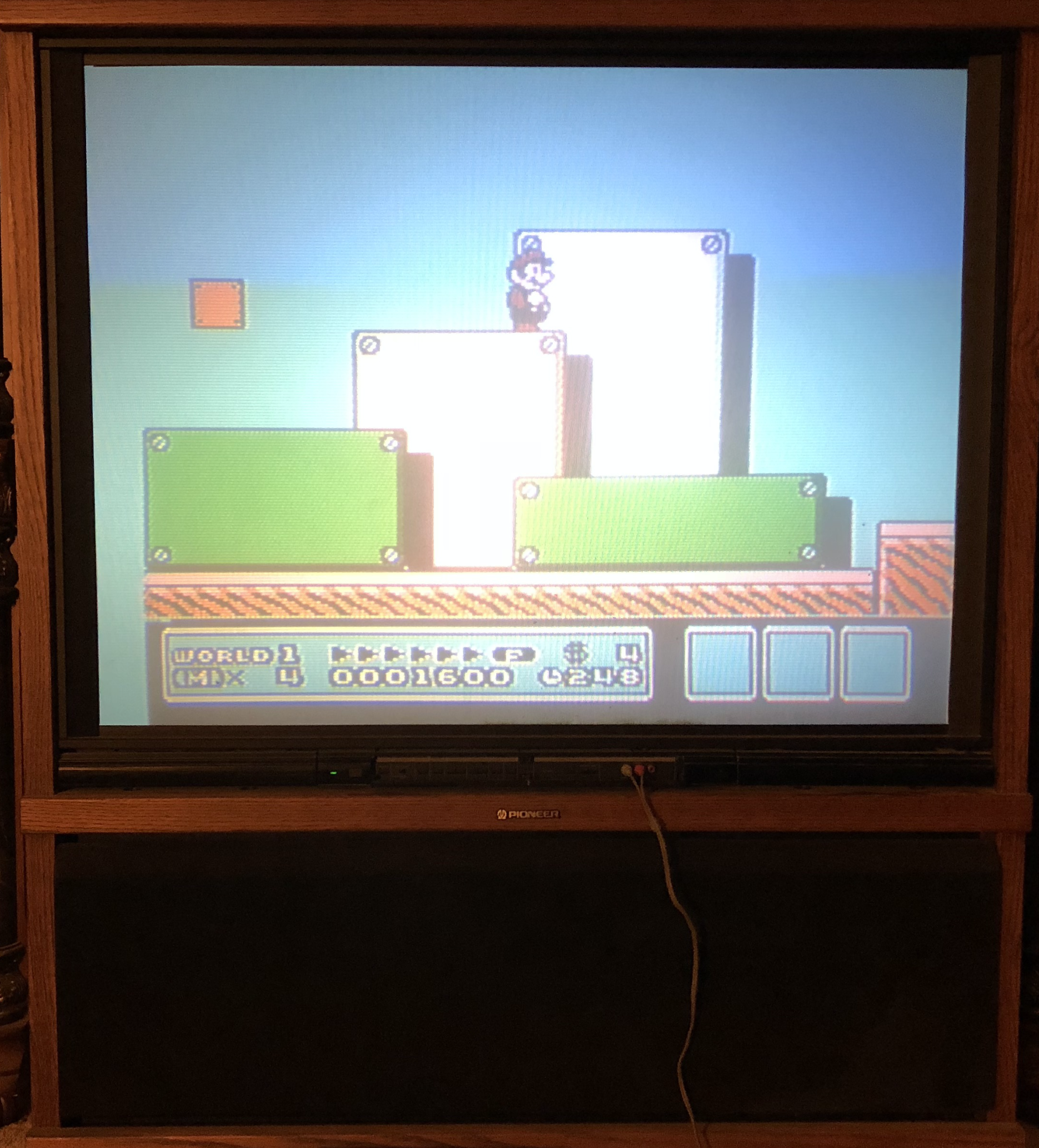
Rear-projection is an obsolete technology used in what was once called “big screen TV”. This Pioneer unit was beginning to show its age:
It is a Pioneer SD-P453S Projection Monitor Receiver, according to the label:

Background
Found the manual: Pioneer SD-P503FP Operating Instructions Manual includes SD-P453FP-Q, and starting on page 27, the SD-P453S. The “S” model adds surround sound. Not many technical details in the operating manual, but it includes a block diagram:

Someone is selling the SD-P453S-Q service manual for $7.99. And another for $4.99, 134 pages Order No. ARP1869 (printed July 1989) for SDP503PQD and related models. I’ll pass, but the preview has this useful diagram on the high voltage generation point, documenting the VR1 ACX1025 variable focus resistor, CRT assemblies, and deflection yokes:

Found a $64.25 repair kit: Pioneer SDP453S & SD-P453S Convergence Repair Kit, but I think this TV has outlived its usefulness. The technology is from the 1980s, or early 90s, time to say goodbye.
Disassembly
Starting with the back panel:

“Pioneer Projection Monitor Receiver Model SD-P453S. AC120Volts 60HZ 255Watts. Pioneer Electronics (USA) INC 2265 East 220th Street Long Beach, California, 90910 USA. Assembled in U.S.A., with U.S.A. and imported parts.” Dolby Laboratories, and U.S. patents:
- 3,632,886 Quadrasonic sound system, filed December 29th, 1969
- 3,746,792 Multidirectional sound system, filed June 15th, 1970
- 3,959,590 Stereophonic sound system, filed July 9th, 1973
SD-P453S-Q, manufactured March 1990. Speaker impedance 8 Ω ~ 16 Ω/speaker. Among the usual warnings are the following: built-in surround processor on/off switch, external speakers left/right terminals, surround balance, audio output variable left/right jacks, control “out” port, two antenna jacks, video/audio input jacks: VDP (and S-Video), VIDEO-1, VIDEO-2, and the same output jacks “REC except video-1”. Zooming out, the rear panel was quite small in relation to the TV, having a large metal grill and black plastic structure:

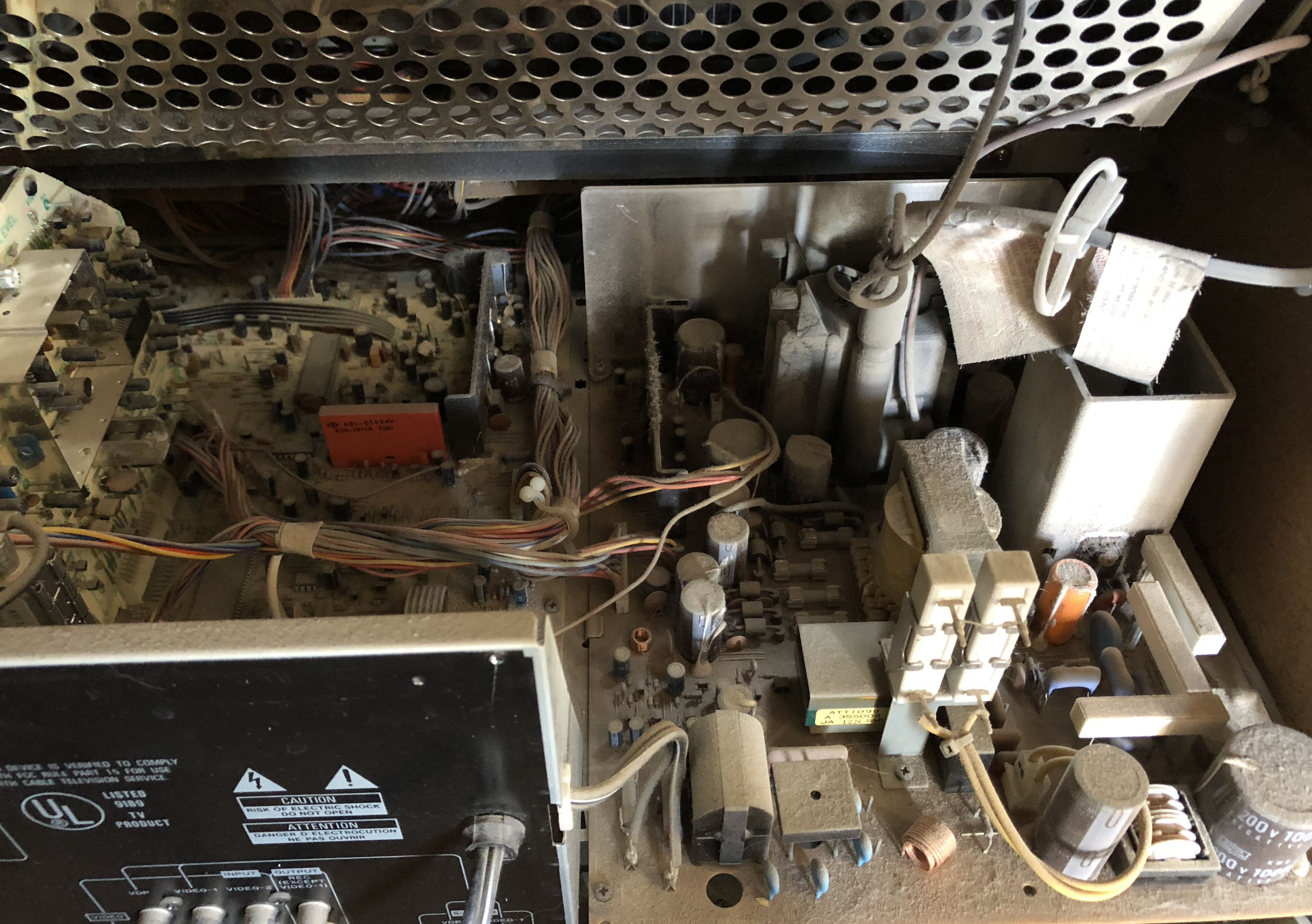
Unscrew the grill. A dusty circuit board is visible, connected to an internal metal mesh:

This is part of the high-voltage power supply. Beware, according to Wikipedia, this HV powering the CRT may be as large as 25,000 volts:
Utilising a 2-inch monochrome CRT driven at a very high accelerating voltage for the size (typically 25 kV), the tube produced an extremely bright picture which was projected via a schmidt lens and mirror assembly onto a semi translucent screen of typically 17 to 19 inches in size.
Closer look, in all its dusty glory. We can now clearly see there are two boards here, power on the right, something else on the left:
Remove the plastic panel on the top, it is an impressively shiny mirror, angled facing the screen. Behind it above the circuit boards are lenses from three miniature CRTs, facing backwards (hence “rear projection”):

Heed the warnings:

“To determine presence of high voltage, discharge anode lead to chassis. High vacuum picture tube is dangerous to handle. Refer servicing to qualified service personnel. This picture tube in this receiver employs integral implosion protection. Replace with a tube of the same type number for continued safety. To reduce the risk of possible exposure to X-radiation, take X-radiation protective measures (see service manual) for personnel during servicing. This product includes critical mechanical and electrical parts which are important for safety”, and here we find the exact magnitude of the high voltage: “This product is 31.4 kV at normal operaton”, wow! Higher than the typical high voltage of RPTVs. Could be useful to someone more adventurous than I, but I’m more interested in the electronic circuitry.
Wiring to the front panel:

beneath it is another label with a diagram showing how the projectors are positioned facing inward, and that they are for red, green, and blue (RGB), in that order.
On the front are two APV1013-A 8Ω E950 speakers with 6.5” diameter:

The system is quite modular, with removable cables between each of the boards. Removing the three small front panel circuit boards, and a shot of the three tubes:

Removing the tubes, a better view of the boards beneath it, and the nice wooden particle case:

Take out the boards, blow them off, and take a look. How many PCBs does it take to build a big screen TV in the 80s? Six or more, apparently:
Boards

From top to bottom, right to left, the main boards are labeled as follows, along with my estimate at their function:
- ANPI306-H: power supply
- ANPI309-B: surround sound, Dolby
- ANPI307-C: IF AGC, video level
- ANPI308-C: adjustments and the biggest heatsink I’ve seen in a while, “convergence board”
- ANPI305-E: main board (also one of the largest I’ve seen in a while), back panel connectors
The -letter suffix may be a revision code, ANPI30X a part code, we have all of: 5, 6, 7, 8, and 9. Looking at each in turn:
ANPI305-E main board
This board is impressively large, measuring 15” x 11.75”. Single-sided. You don’t seem them this large much anymore. When I enter the dimensions in PCBShopper to get a ballpark quote, it warns me: “You have requested a size of 15 x 11.75 inches. That seems unusually large. Do you want to continue?”. In small quantities, getting a board of this size manufactured may set you back over a hundred dollars. Must have been worth it back then, I guess. Barely fits on the bench, these are the best shots I could get of it (and these photos were too big to upload here so I had to resize, bear with me):

The printed side:

Looking at some of the DIP chips:
- PA0040 9KC 110 - unknown, Pioneer ROM?
- AN5302K 9N7 - Panasonic NTSC Luminance Signal, Chroma-Signal and Synchronous Signal Processing
- Toshiba TC4066BP 8951HB JAPAN, part of the 4000 series, Quad Bilateral Switch, PDIP14
- NEC JAPAN D6145C 001 8928DK, found a replacement on eBay: D6145C 18-PIN INTEGRATED CIRCUIT, but couldn’t find a datasheet
- 80011A 9463 - Aliexpress had a similar chip labeled 80011AA 1371 but didn’t describe what it is, if its a Mitsubishi M6M80011AP, then it could be a 1024-bit (64-word by 16-bit) electrically erasable and programmable ROM, “suitable for nonvolatile channel memory for electronic tuner”
- Pioneer 9H1 PDG040 5048H-197, probably a parallel ROM, an eBay seller is asking $39.95 for it
- Toshiba TC4051BP 8952HB JAPAN (2x) - Single 8-channel multiplexer/demultiplexer
- PA0030 9K1 116 - another Pioneer chip, this also makes an appearance in the Pioneer PDP-501MX Plasma Television, whose technical manual is available (PA0030 is IC9961 there) and is used for sharpness control
- T TA7630P - Toshiba Dual Volume/Balance/Tone Bass/Treble DC Control IC
There are also 3-pin linear voltage regulators: a 78M09A (IC601, 9 volts), and 78M05 (IC206, 5 volts). The chip in the HZIP-12 package with the big heat sink is a Toshiba TA8200AH Dual Audio Power Amplifier. This thing has some big speakers, no wonder it needs a big amplifier. Other interesting parts are the brown lumps labeled ATNI1013-A (two of them) and ATNI1014-A, and the large orange box labeled ADL-CT03AU ATN-101A 1907, possibly some radio components? Inductors?
From this an APNI307, scored a few linear voltage regulators, two 7809’s and one 7805:

The date codes indicate these were manufactured in 1990 and 1989, respectively.
I’d like to try dumping the EEPROM, if that’s what it is. 80011A is an 8-pin DIP. Is it the M6M80011AP detailed in 1024-bit (64-word by 16-bit) electrically erasable and programmable ROM? From the data sheet:

Wired up to a Bus Pirate 3.6 as follows:
| 80011A | Bus Pirate | Remarks |
|---|---|---|
| 1 (/CS) | CS | Chip select |
| 2 (/SCK) | CLK | Clock |
| 3 (DI) | MOSI | Slave input |
| 4 (DO) | MISO | Slave output |
| 5 (Vss 0V) | GND | Ground |
| 6 (RESET) | (wire to /CS) | “This pin and /CS can be interconnected” (pg. 3-4) |
| 7 (RDY /BUSY) | AUX | Busy output |
| 8 (Vdd 5V) | 5V | Power |
The data sheet doesn’t use the term SPI, but it says “M6M80011AP is a clocked serial port compatible EEPROM, and data is input from the rising edge of the clock signal and output by synchronizing to the falling edge of the clock signal.” On the Bus Pirate, type m and 5 to select SPI, go with a conservive 1 30 kHz, 1 clock polarity idle low (default), 1 output clock edge active to idle (default), 1 input sample middle phase, 2 chip select /CS active low (default), 1 output type open drain.
The read command is 0b10101000, followed by the 8-bit address. 16-bit words. Turn on the power with W thentTry to read the first word:
SPI>[0b10101000 0 rr]
/CS ENABLED
WRITE: 0xA8
WRITE: 0x00
READ: 0x00
READ: 0x00
/CS DISABLED
SPI>
There are 64 words, surely some must be non-zero. What’s the problem? For starters, this is a 5 volt part but the Bus Pirate outputs 3.3 V. To solve this, interfacing with non-3.3 chips, the Bus Pirate can output open drain, see: Hackaday: Mixed voltage interfacing with the Bus Pirate. Connect the voltage pull-up (VPU) to 5V, then enable pull-ups with P, now it reads all 0xFFFF’s:
SPI>[0b10101000 0 rr]
/CS ENABLED
WRITE: 0xA8
WRITE: 0x00
READ: 0xFF
READ: 0xFF
/CS DISABLED
No such luck. This chip may be something else than EEPROM, I may have damaged it, or hooked it up wrong. This was my setup:

ANPI306-H power board
Moving onto the next board, the grimiest of them all. Made some effort to clean it up, but a lot of dust stuck to this board and was covered in oil dripping from the lenses, and its the board with the chunkiest components making it difficult to clean. Almost considered discarding it, but the parts will be easier to clean after removal from the board. Brace yourself, here is this dirty PCB:
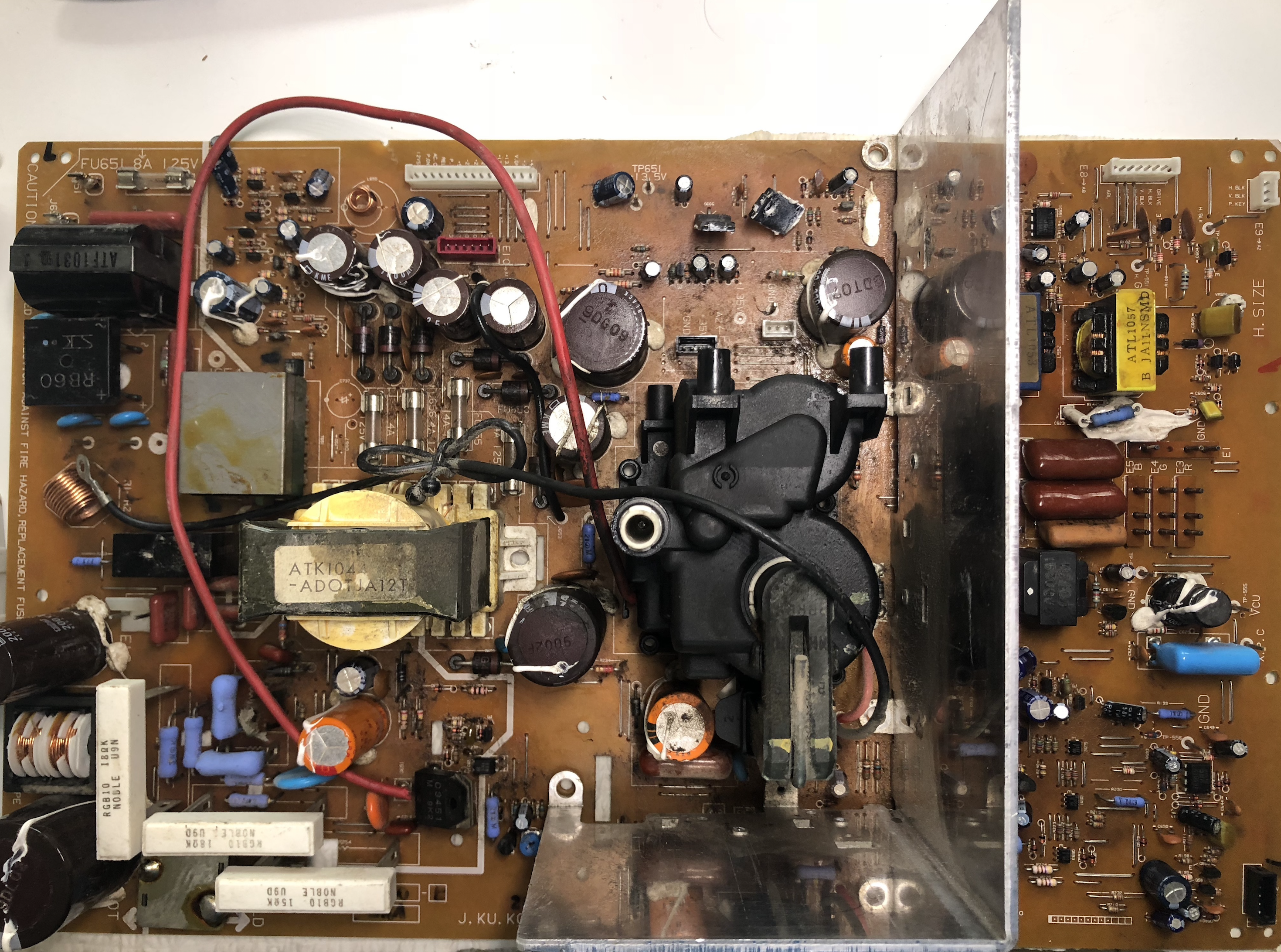
The other side is cleaner:

This board is serious business, check out those fat traces for high voltage on the hot side. Power resistors made out of cement. A thick aluminum heat sink cornering the transformer. Off the board, but nearby, are two 0.47Ωk (not kΩ, I measured - this is milliohms not kilohms) RGB20 NOBLEU9D cement resistors in series. Lots of fuses. The big capacitor in the corner is a 200V 1000µF Nippon Chemi-Com. Predating the capacitor plague of 1999-2007, this capacitor and the others like it (a 200V 560µF nearby) are still good.
Close by is an Omron relay, G2R-1117P-FD-V-US-PN 12VDC, contact: TV-8 10A 250VAC or 10A 30VDC. The tiny transformer is labeled ATT1099 A 35S008 JA 12N SMD, the medium size transformer ATK1044 -ADOTJA12T. Bridge rectifier labeled RB60 SK with +, -, and two ~ terminals. ATF1031 9D J, a current transformer? The flyback transformer has no labels immediately visible, and on the other side are four more even smaller transformers: ATL1058 A SMD (blue), ATL1057 B JA11NSMD (yellow), 260291 8947M (black), and 2250291 8947M (black). There are few integrated circuits, a few transistors here and there. Notable ICs:
- 4558DX JRC (2x), IC552_5 and IC551, DIP-8 - JRC558 dual operational amplifier
Not my favorite board.
ANPI307-C RF board
Back to something more manageable. The ANPI307-C is clearly related to RF, there were two metal shields over components, I removed:
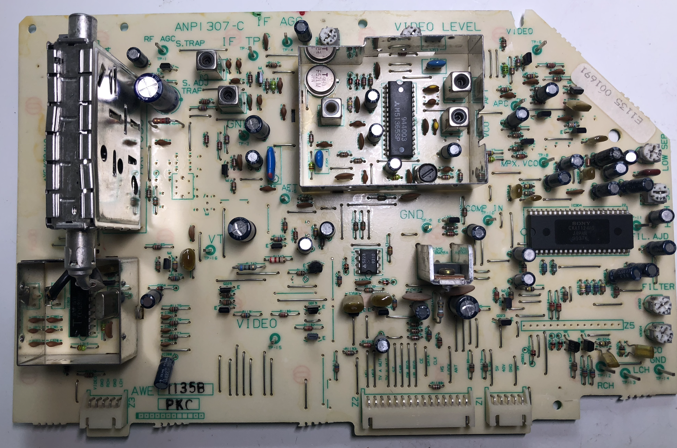
Other side:

- Toshiba TD6359P 9 J 611 - Frequency Synthesizer for TV/CATV
- 944003 M51365SP - Mitsubishi PLL-split VIF/SIF, “consisting of an IF signal processor for color TV sets… circuits include VIF amplifiers, video detector, VCO, APC detector, AFT, video equalizer, plus IF/RF AGC and SIF detector functions”, lots of TV-related RF stuff here
- 4.00 NDK99 crystal
- Toshiba F52LM 9H3 JPN - in a metal can, “Active Filter for Telecommunications - TV-IF Saw Filter, 45.7 MHz carrier, adjustment free”, maybe useful for radio hobbyists? Surface Acoustic Wave filters, an analog implementation of a FIR filter.
- Mitsubishi 5223 9210 Dual Single Power Supply Operational Amplifier, DIP mini flat
- Sony CXA1124AS JAPAN 9G37K - US Audio Multiplexing Decoder IC, “designed for the MTS decoding systems. This device contains a stereo signal demodulator, a SAP (Second Audio Program) signal demodulator and dbx-TV noise reduction decoder. The Main 100% reference input level of the CXA1124 (CXA1534) is 245mVrms (100mVrms).”
The crystal’s leads are behind a metal shield, desoldered it then desoldered the crystal. For some reason the crystal had longer leads and they were bent in a zig-zag (were the long leads picking up interference so they put a shield over it instead of cutting them?). Tested the crystal in a frequency tester, expecting 4 MHz. But it only read zero, unclear why (damaged?).
Not much generically useful here, but it does have some trimmer pots. Moving on.
ANPI308-C convergence board
Speaking of trimmer pots, this board has 32 of them, ought to be enough for anybody:

The DIP chip is a Pioneer PA0036 9LC 111, sold on eBay for $8.95, brand new, “used in various models”, but it doesn’t say what it is. Given the adjustment labels:
| GV | RH | RV | BH | BV | |
|---|---|---|---|---|---|
| TP-702 | VR709 | VR718 | VR75 | VR734 | SKEW /// |
| VR709 | VR710 | VR719 | VR726 | VR735 | BOW ))) |
| VR706 | VR711 | VR720 | VR727 | VR736 | KEY \\|/ |
| VR707 | VR712 | VR721 | VR728 | VR737 | SUB KEY |
| VR708 | VR713 | VR722 | VR729 | VR738 | PIN (\|) |
| VR714 | VR730 | SUB PIN |
|||
| VR715 | VR723 | VR731 | VR739 | LIN \|->\|-> |
|
| VR716 | VR732 | SUB LIN \|<-\|<-\|->\|->\| |
|||
| VR717 | VR721 | VR733 | VR740 | SIZE \|<-\|->\| |
I’d say it is related to video. The three SIPs, for red, green, and blue, are Mitsubishi M5220L 9702, more opamps: Dual Low-noise Operational Amplifiers (dual power supply type). Of course, the elephant in the room is that big heat sink over there. What’s under it?

Labeled “STK4277 SL OA 18”, and much of the board connects to it. Pioneer has it on their website, not available but says retail price $75.25: PART DETAILS - STK4277-SL. Found a post from someone trying to replace this part in 2004, fone.freaky asked on electronicspoint forums, Convergence still off after replaced STK4277 in Pioneer 6081 tv, John Del replied:
The STK is just the amplifier, you need to scope the error correction waveform inputs that come from the ramp generator section.
The STK4277-SL is a replacement for the $80 STK4729-SL. Found a cached page on Aliexpress (mirror), selling it for $8.90 as “STK4279:2 Channel AF Power Amp”. Newegg has 50 for $217.33. eBay has it for $5.95. bdent calls it a “5-channel Convergence Correction Circuit IC for video projectors”, a SIP-25 convergence IC. Amazon for $22.
Couldn’t find the exact data sheet, but we know it is a 5-channel convergence correction power amplifier. Found the STK4145MK2 data sheet, maybe not too dissimilar. Can this chip be usefully used in another circuit?
ANPI309-B audio board
Moving into the final stretch, this board is for audio, indicated by the “Dolby Level Adjust” text:


Were Single Inline Packages (SIP) more common back then? This board has several, as well as some DIPs. Or actually, they are ZIP, Zig-zag in-line packages. List:
- BU4066BL (2x) (IC510, IC508) - Quad Analog Switch, but in ZIP-14
- Mitsubishi M5222L - Dual VCA for Low Voltage Electronic Volume Control, SIP-8
- Sanyo LA2730 - Dolby B-Type Noise Reduction System
- Mitsubishi M5218L - Dual low-noise operational amplifiers (dual power supply type)
- Sanyo LM3364K, $6.95/10 on eBay reveals this is RAM: SANYO LM3364K-15 Dynamic RAM Gated RAS-Only Refresh 16-Pin Dip Qty-10
- Mitsubishi 944002 M50199P Mitsubishi Sound Processors M50199P Digital Delay
- Mitsubishi M5233 9701 (IC502_5), discussion. This is a Dual Comparator, “a differential circuit which is equivalent to a conventional single power supply operational amplifier”, voltage range from 2 to 36V.
Could be an interesting project to try using the DRAM somehow. dmitry.gr’s Linux on an 8-bit micro? used a 30-pin SIMM memory module, refreshed every 62 ms, driven from an ATmega644a, for a maximum bandwidth of 30 KB/s. Could the Sanyo LM3364K dynamic RAM be driven in the same way? But I had trouble finding a data sheet, and it is not clear that’s even what this chip is.
Front panel boards
Not much to these, buttons and jacks. There’s a lot of good switches here, I desoldered one but it took too long, taking them all off would best wait for a hot air gun. But the cadmium sulfide CdS photoresistor is worth salvaging. I measured about 15 kΩ resistance in ordinary room lighting, and about 5 kΩ under a bright lamp.


The RF adapter is actually not part of this TV, but was a separate unit labeled “Dreamcast Model No. HKT-8820 NTSC-M CH3-CH4”, with ANT.IN antenna input, TV output, A/V IN, and a select channel 3 or channel 4 switch:

Dreamcast was a 1999 home video game console. This adapter was used to allow the TV to pickup the video game console on analog TV channel 3 or 4:
A channel 3/4 output was a common output selection for consumer audiovisual devices sold in North America that were intended to be connected to a TV using a radio frequency (RF) signal. This channel option was provided because it was rare to have broadcast channels 3 and 4 used in the same market, or even just channel 3 itself. The choice allowed the user to select the unused channel in their area so that the connected device would be able to provide video and audio on an RF feed to the television without excessive interference from a broadcast signal.
Bend away the metal shields, and parts can be desoldered from the boards. Nothing terribly interesting, but the color-coded inductors look kinda cool, they came in red, green, and blue:

Memories of Analog TV: The 90s and 00s provides some insight into the old analog era. Nowadays, it is largely superseded by digital televison, analog services turned off as part of the digital television transition. Receiving modern television on this big screen would have required a digital television adapter. Better to buy a new TV.