blog
Powerful Function LTCMD720NIR CCD Camera teardown
by snm, January 28nd, 2018
Unboxing and manual
Came in a box labeled “Powerful Function - CCD Camera”:

The short manual says it is model LTCMD702NIR, featuring a 1/3” Sony Super Had CCD, with 480 TVL, 0 LUX, 3.6mm lens, and powered with 12VDC, emitting an NTSC video signal:

A closer look at the end of the manual since I couldn’t fit it all in my camera:

Under the cover
Unscrewing the protective cover, we see the camera assembly:

It is affixed to the body with two screws. Remove them and the camera comes right off:

The power and video cable can also be unplugged from the socket. Next step, take apart the mounting brackets:

And finally, the adjustment arms:

Plenty of screws and washers for the taking. But the triple stacked PCB design is pretty interesting. Let’s take a closer look.
Unstacking the PCBs
The camera viewed head-on:

It is screwed to the top board, the power/video plugs into the bottom board, and there is a third board in the middle. Presumably the top is for interfacing to the camera, and the bottom is for the power supply. Easily taken apart by removing the corner screws and standoffs:

Power board
This is the bottom-most board the external cable plugs into. A large capacitor, and small transformer, definitely related to power. The silkscreen label reads “DUAL BOARD 04/07/06”. A few large SMD diodes, capacitors, and a fuse. DIP switches per the manual. The transistor in the middle is a Fairchild IRFR224B, a 250V N-channel MOSFET:

The other side of the board has some diodes, passives, and connectors for stacking to the board below:

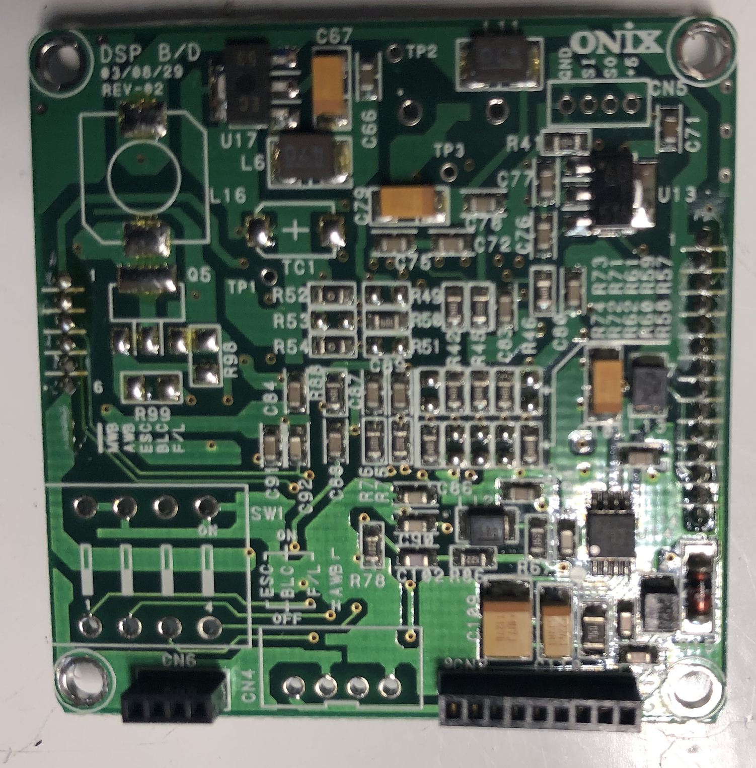
Signal processing board
The middle board (silkscreen labeled “ONIX”) is more intricate, it contains a chip labeled Sony CXD2163BR 519L57V:

and the other side, whose silkscreen “DSP B/D” gives away its function, digital signal processing:
Found the Sony CXD2163BR data sheet, which says it is a “Signal Processor LSI for Single-Chip CCD Color Camera”, in a 100-pin LQFP, with a built-in microcontroller:
The CXD2163BR is a signal processor LSI for Ye, Cy, Mg and G single-chip CCD color cameras. In addition to basic camera signal processing functions, it includes an AE/AWB detection circuit, a sync signal generation circuit and an external sync circuit, etc. This chip also has a built-in microcontroller to realize basic camera functions without a microcomputer. The CXD2163BR is a fully improved version and pin compatible with the CXD2163R by adding some functions and improving its performance.
A sophisticated block diagram:

and pinout:

very application-specific, probably not much use outside this application, although the built-in microcontroller may be interesting to get up and running on its own. Onto the next and final board.
CCD board
This is the printed circuit board the camera screws into:

Several chips, related to the CCD camera as we might expect:
- Sony A2006Q 513 E03V - Digital CCD Camera Head Amplifier
- Sony D2480R 513 B83N - Timing Controller IC with Built-in CCD Driver
- 3414A 519V JRC - Single-Supply Dual High Current Operational Amplifier
Again quite application-specific, but repurposing the opamp could be interesting. Opamps were also very common in a previous teardown, Pioneer SD-P453S Rear-Projection (RPTV) teardown: inside an 80s vintage big screen TV.
Flipping it over, after removing the camera lens, the camera itself:

The silkscreen says “CCD BOARD REV-02”. The chip on the top is 88347 E10506 M38, I couldn’t find much information for but it may be a digital-to-analog converter.
Conclusions
Stacked the boards back together:

The stacking board design allowed the designers of this product to fit all of the needed circuitry into a few square inches beneath the camera mount, all inside a convenient enclosure. Not bad. There is however for better or worse not much too salvage from this device, since it is highly integrated.